Hyperbole fails me when trying to describe the importance of computer chips to the world today. Everything made possible by computers relies on chips. Chips rely on transistors. Transistors rely on silicon. Silicon relies on Lithography.
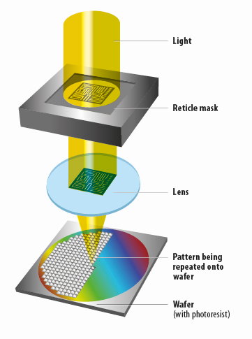
Lithography the process of putting an image onto the surface of the silicon. Pretty much like the way a silkscreen puts “Team Building Exercise 1999” on a T-shirt. Except that this image has to be the highest resolution, with the smallest microscopic features, of anything humans produce.
“Moore’s Law” usually refers to increasing transistor density. Basically, how can we make transistors half as big as they were 18 months ago? Every time we figure that out, computers get twice as powerful.
The state of the art uses Extreme Ultraviolet (EUV) light to do the lithography. The machine that can do this cost $50 billion to develop. It has 500,000 parts. Only the Large Hadron Collider is more complicated. To buy one costs $250 million and you’ll be stuck on a waiting list that is $40 billion long. The machine comes from ASML in the Netherlands and they don’t have a single competitor, in the entire world.

That machine shoots a tiny ball of molten tin into a vacuum and blasts it with two lasers. This produces a flash of 13.5 nanometer ultraviolet light that gets aimed at the surface of a silicon wafer. You are looking at the pinnacle of human engineering achievement. Now you know how the chip for your iPhone is made.
ASML advanced from 193nm to 13.5nm light to make this possible, but there’s a problem. The diffraction limit of 13.5 nanometer light was set by either God or Issac Newton and there’s nothing we can do about it. We can’t print features smaller than that and there’s no practical way to do lithography with a shorter wavelength. When people say that Moore’s Law is over, this is why. We can’t keep making smaller transistors.
The semiconductor industry knows this, so they’ve tried to solve the problem by handing it over to the marketing department where the laws of physics don’t apply. You’ve seen them progress from 45nm to 30nm to 20nm over the last decade, then all of the sudden, 12nm, 7nm, 5nm & soon 3nm chips are coming. Well guess what, it is all just marketing bullshit.
This measurement in chips used to be half the distance between the centers of two features. Once marketing took over, they started measuring half the distance between the edges of two features. Instant improvement! Then they started measuring other random stuff. Other kinds of improvements in chip design helped to gloss over the fact that we are no longer able to shrink the size of transistors by 50% every 18 months anymore.
Today, there are extraordinary geopolitical machinations to control chip production. The U.S. has new tariffs and export controls akin to those for fighter jets and ICBMs (both are largely made of chips anyway). Access to chip production is as critical to superpowers as oil.

Lace Lithography use helium atoms instead of ultraviolet light to etch features onto silicon. The beam Lace will use to make chips is about the width of a single helium atom, or 0.1 nanometer. This is the only known technology that can go well beyond Extreme UV and put Moore’s Law back on track. ASML is worth over half a trillion dollars. Lace Lithography will be their successor.
Along with Vsquared, Runa & Future Ventures, we are their first investors.
